Ent: Design your own custom keyboard
This will be a walkthrough on how I made my own custom keyboard, starting from complete beginner in PCB design software, keyboard design, etc.
The keyboard’s code and everything related to it can be found here.
> fzf old keyboards
My first split was Mitosis, a 46 key split wireless keyboard based on nRF51822, a Bluetooth-enabled microcontroller, which was used for communication between the two halves and the receiver that was eventually connected with the host.

- The keyboard being battery powered, I had to buy, replace and carry with me CR2032 batteries (non-rechargeable) all the time.
- Most of the thumb cluster keys were extremely difficult to hit.
- The keyboard’s profile (height) was a bit too high, leading to me raising my fingers/hands too much.
- The pinky column was not
stagerredenough for my hands (more on what that means later).
KiCad
At some point I stumbled upon a YouTube video from Ben Vallack called Design Your Own Keyboard, which is about creating a keyboard from scratch. I immediately got the idea of creating my own as well, following that process.
The first piece of the puzzle, is KiCad, an open-source electronics design software that you can design your own PCBs on. I must admit that compared to other design software (e.g. Blender, FreeCAD) KiCad was relatively easy to navigate.
Ergogen
Ergogen is an awesome project that aims to make it easy to prototype a new keyboard even if you don’t know -almost- anything about PCB design, and iterate on keyboard designs.
In essence, you describe the keyboard in JavaScript code and Ergogen produces a KiCad file containing
the PCB. Ergogen
provides all the commonly-used keyboard components,
such as: keys (MX, choc, etc), microcontrollers, rotary encoders
as KiCad footprints.
The design
After contemplating a lot what I want on my keyboard (how many keys, rotary encoders, trackpads etc), I got a friend interested in it, and we came up with the following features:
Wired split keyboard: reduced complexity compared to wireless and we won’t have to mess with batteries and wireless communication protocols.Reversible: meaning that the left and right halves of the keyboard come from the same PCB, on one side you got the left keyboard half and on the other the right half. This will cut down on manufacturing costs since we won’t have to print separate left and right PCBs.Trackpad: we wanted a small trackpad on the keyboard for most simple mouse needs.Hotswappable keys: Instead of soldering the key switches directly on the board, you can solder a hotswappable socket on the board and insert the key switch on them. This makes replacing a key switch as easy as pulling them out.Underglow LEDs: Add LEDs on the bottom side of the keyboard.Aggressive pinky stagger: to overcome the problem I had with Mitosis, I wanted the pinky column, to be lower than the rest of the keyboard columns. This made it easier to hit keys.Distant thumb keys: Most, if not all split keyboards, put the thumb keys close to the main keyboard body, leading to your hand becoming a claw to use it. This always felt uncomfortable to me, so I put it lower than usual, away from the rest of the keyboard.
A glimpse on the design as code
points:
  zones:
    matrix:
      columns:
        pinky:
          key:
            origin: [0, -17]
            spread: spread
          rows:
            bottom:
              bind: [5, 0, 0, 1]
              column_net: IO21
            home:
              bind: [0, 12, 0, 1]
              column_net: IO16
            top:
              bind: [0, 8, 5, 1]
              column_net: IO15
[...]
This excerpt defines a new keyboard column along with the column_net for each
key which basically dictates that each key should be connected to a specific IO pin
on the microcontroller.
Finalize the PCB
After a lot of iterations between Ergogen and KiCad, the only thing left to do is routing, in other words create the actual PCB traces connecting the various components. This process can be automated to some extent, but after trying auto-routing solutions I was disappointed and resorted to manual routing. Doing the routing manually felt like an odd art (wax on, wax off) despite it being tedious to find the right path for component and make everything look nice as well.

Tooling review
Ergogen turned out to be a helpful tool for a beginner, since you can iterate on your idea quickly without getting really into KiCad yet, until you get to the routing step that’s done entirely on KiCad. On the other hand, Ergogen has its own learning curve and terminology, and arguably for a single keyboard one could go straight to KiCad for the development.
Also, as mentioned above Ergogen simply generates a single kicad_pcb file that contains all the components you have described in code, but it essentially forces you to some bad practises such as not creating a schematic for your PCB. The regular KiCad design process begins with a schematic (describe visually all the components’ connections) and then you jump over to creating the PCB itself (where components should be spatially)
As for KiCad, I’ve been amazed by how easy and intuitive it was to use it, correct mistakes using KiCad’s DRC feature, route, hop between schematic and PCB.
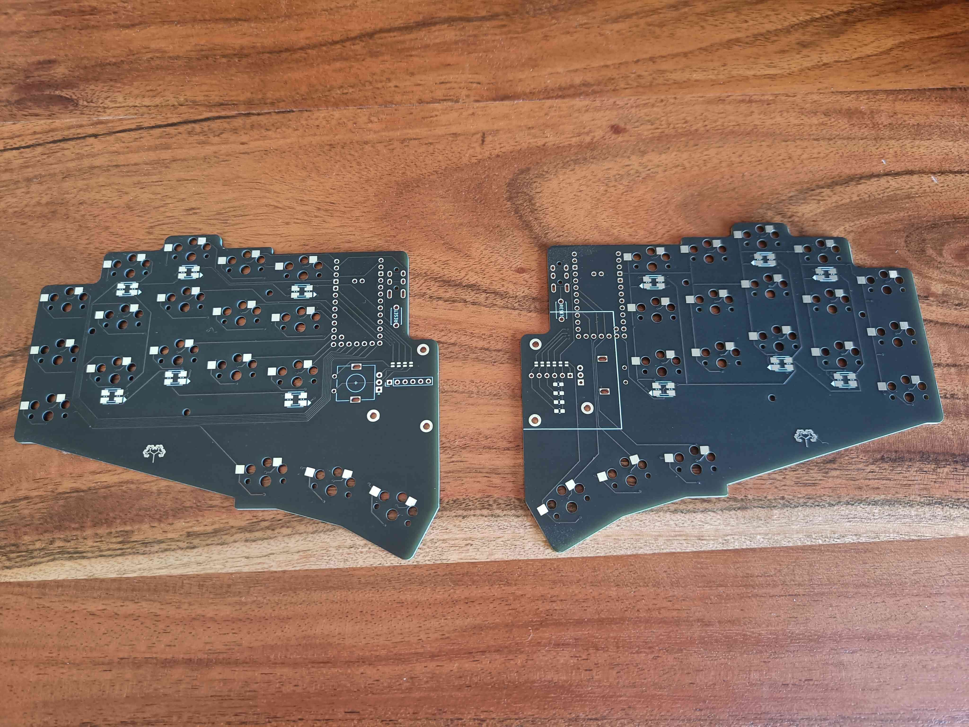
Manufacture the PCBs
I used an overseas PCB manufacturing service that took about 3 weeks (!) in total (shipping included), which is mind blowing considering the complexity of the manufacturing process, and the fact that you can send any design, with any kind of complexity you want to be printed (following the factory’s guidelines of course)
The factory takes in your gerber files (KiCad outputs this format), describing the PCBs you want to manufacture, their engineers are going over them to spot any easy mistake/violation or anything that’s not aligned with their manufacturing guidelines.

Solder and assemble the thing, et voila
This final step involves some soldering of the various components, designing a 3D printed case (Ergogen also does this bit for you), and putting everything together.

Was it worth it?
Absolutely. The process of designing and developing the keyboard was a blast and it was surprising how easy it was to get started with all the tools one needs to get this done. Also, the keyboard turned out to be a perfect beginner PCB to design, since you basically just need to route the switches to a microcontroller (plus some extra bits for the split communication, trackpad etc).
A natural downside coming from the software world is that iterating on PCBs takes both time and money to manufacture each version of it. Thankfully, I got it right the very first time I manufactured my PCB.
Overall it was nice to delve into how something so basic, that’s been around for so long, such as a keyboard works, take it apart and make my own. The keyboard I came up with is designed around what I want from it and fits my hands exactly.
I have been using this keyboard as my daily driver for a long time, improving my WPM counter (currently I’m at around 80 WPM), and it really feels comfortable on my hands. I’m already preparing for the 2nd version of it 🥁!